Wafer Metal Plating Service Market Forecast to 2034 Shows USD 3.41 Billion Opportunity at 6.7% CAGR
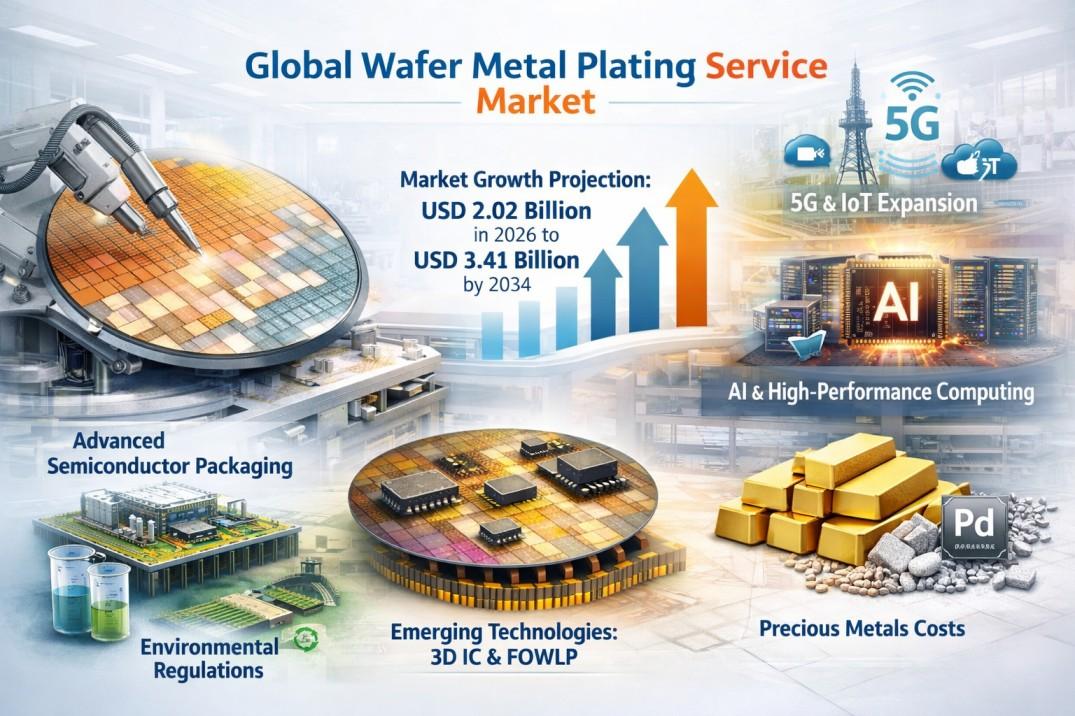
According to a new report from Intel Market Research, the global Wafer Metal Plating Service market was valued at USD 1.85 billion in 2025 and is projected to grow from USD 2.02 billion in 2026 to USD 3.41 billion by 2034, exhibiting a robust CAGR of 6.7% during the forecast period (2026–2034). This growth is propelled by increasing demand for high-performance semiconductors in AI applications and 5G infrastructure, coupled with advancements in fan-out wafer-level packaging technologies and the continued push toward finer pitch interconnects in advanced microelectronics manufacturing.
What is Wafer Metal Plating Service?
Wafer metal plating services involve the deposition of thin layers of conductive metals onto semiconductor wafers through electrochemical or electroless processes. These services are critical for manufacturing integrated circuits, MEMS devices, and advanced packaging solutions, enabling electrical connectivity and improved performance in microelectronics. Key plating materials include copper, gold, nickel, and silver, each selected based on conductivity requirements and application-specific needs. The industry serves a broad spectrum of end users, from large-scale foundries and integrated device manufacturers to outsourced semiconductor assembly and test providers.
This report provides a deep insight into the global Wafer Metal Plating Service market covering all its essential aspects-from a macro overview of the market to micro details such as market size, competitive landscape, development trends, niche markets, key drivers and challenges, SWOT analysis, and value chain analysis.
The analysis helps the reader understand competition within the industry and strategies for enhancing profitability. Furthermore, it provides a framework for evaluating and accessing the position of a business organization. The report also focuses on the competitive landscape of the Global Wafer Metal Plating Service Market, introducing market share, performance, product positioning, and operational insights of major players. This helps industry professionals identify key competitors and understand the competition pattern.
In short, this report is a must-read for industry players, investors, researchers, consultants, business strategists, and all those planning to foray into the Wafer Metal Plating Service market.
📥 Download FREE Sample Report:
Wafer Metal Plating Service Market - View in Detailed Research Report
Key Market Drivers
1. Growing Demand for Advanced Semiconductor Packaging
The wafer metal plating service market is experiencing significant growth driven by the surge in demand for advanced semiconductor packaging solutions. With the increasing miniaturization of electronic components, manufacturers require high-precision wafer metal plating to enable smaller, more powerful chips. Leading players such as PacTech and JCET Group are actively expanding their plating capabilities to address the growing need for finer pitch interconnects below 10μm, a threshold that is becoming standard for next-generation logic and memory devices. This evolution in packaging complexity is creating sustained demand for precision plating services across the global semiconductor supply chain.
2. Expansion of 5G Networks and IoT Ecosystems
The global rollout of 5G networks and the proliferation of Internet of Things devices have created substantial and sustained demand for wafer plating services. These technologies require specialized metal plating for high-frequency applications, where signal integrity and thermal management are paramount. The resulting need for ultra-thin, highly uniform metal deposits has elevated the importance of advanced electroplating and chemical plating techniques. Automotive electrification represents an additional high-growth driver, with wafer plating services being increasingly critical for advanced driver-assistance systems (ADAS), power modules, and vehicle electrification components that demand high-reliability metallization.
3. Accelerating AI and High-Performance Computing Demand
The rapid expansion of artificial intelligence workloads, data center infrastructure, and high-performance computing architectures is driving unprecedented demand for advanced semiconductor packaging. Wafer metal plating services are integral to enabling the copper interconnect layers, redistribution layers, and bump structures required for chiplet-based designs and 2.5D/3D IC integration. As hyperscalers and semiconductor manufacturers invest heavily in AI accelerator chips, the downstream demand for sophisticated plating solutions is expected to intensify throughout the forecast period.
Market Challenges
- Stringent Environmental Regulations – The wafer metal plating service industry faces growing compliance burdens related to chemical usage and wastewater management. Increasingly strict environmental standards in major manufacturing regions add significant operational costs and require ongoing investment in effluent treatment and process optimization.
- High Capital Investment Requirements – Establishing and maintaining wafer plating facilities requires substantial capital expenditure for specialized equipment, advanced process chemistries, and cleanroom environments. These elevated barriers to entry limit the pace at which new service providers can emerge to meet growing market demand.
- Skilled Labor Shortage – The industry faces persistent challenges in recruiting and retaining technicians with specialized knowledge in semiconductor-grade plating processes. As technology nodes advance and process windows tighten, the requirement for highly trained personnel becomes even more critical.
Market Restraints
Fluctuations in the prices of precious metals used in wafer plating-particularly gold and palladium-create pricing challenges for service providers. This volatility complicates long-term contract negotiations and places pressure on profit margins, particularly for providers serving applications that mandate gold-based finishes for reliability and corrosion resistance. Managing raw material cost exposure through hedging strategies and material substitution is becoming an increasingly important operational discipline for market participants.
Emerging Opportunities
The growing adoption of Fan-Out Wafer-Level Packaging (FOWLP) technology presents one of the most significant near-term opportunities for wafer metal plating service providers. This advanced packaging approach requires specialized plating solutions for redistribution layers, creating new revenue streams and differentiating capabilities for providers with deep process expertise. Beyond FOWLP, the transition to larger wafer formats-particularly 300mm-and the integration of compound semiconductors into mainstream packaging are opening additional avenues for growth. Key opportunities across the market include:
- Expansion of advanced packaging service capabilities for chiplet and heterogeneous integration architectures
- Development of novel alloy plating chemistries tailored to specific thermal and electrical performance requirements in 3D IC applications
- Investment in sustainable and green plating processes to meet tightening environmental regulations while maintaining competitive cost structures
- Strategic capacity expansion in Asia-Pacific, North America, and Europe to serve regional semiconductor fab buildouts
Collectively, these developments are expected to accelerate innovation, attract new investment, and expand the addressable market for wafer metal plating services across geographies and end-use applications.
📥 Download FREE Sample Report:
Wafer Metal Plating Service Market - View in Detailed Research Report
Regional Market Insights
- Asia-Pacific: Asia-Pacific dominates the global wafer metal plating service market, driven by the high concentration of semiconductor fabrication plants in Taiwan, South Korea, China, and Japan. The region benefits from continuous government support for semiconductor self-sufficiency, frequent capacity expansions in wafer fabs, and the presence of major OSAT providers that generate strong downstream demand for plating services.
- North America: North America maintains strong capabilities in specialized wafer plating services, particularly for defense, aerospace, and high-performance computing applications requiring high-reliability metallization. The region benefits from close collaboration between plating service providers and fabless semiconductor companies developing innovative chip architectures, and is seeing renewed investment driven by domestic semiconductor manufacturing initiatives.
- Europe: Europe's wafer metal plating service market is centered on automotive and industrial applications with stringent quality requirements. German and French plating specialists are leading in the development of environmentally sustainable processes compliant with EU regulations, with growing activity in power semiconductor plating for electric vehicles and renewable energy systems.
- Latin America and Middle East & Africa: These regions remain in early stages of wafer plating market development, with most services currently imported. However, strategic investments in semiconductor infrastructure across Gulf nations and Brazil's emerging electronics manufacturing base are expected to create incremental opportunities over the forecast horizon.
Market Segmentation
By Type
- Electroplating
- Chemical Plating
- Others
By Application
- Semiconductor
- LED
- Others
By End User
- Foundries
- IDMs (Integrated Device Manufacturers)
- OSATs (Outsourced Semiconductor Assembly and Test)
By Plating Material
- Copper
- Gold
- Nickel
- Others
By Wafer Size
- 200mm
- 300mm
- Others
By Region
- North America
- Europe
- Asia-Pacific
- Latin America
- Middle East & Africa
📘 Get Full Report Here:
Wafer Metal Plating Service Market - View Detailed Research Report
Competitive Landscape
The wafer metal plating service market features a dynamic mix of specialized semiconductor material providers and precision plating technology specialists. PacTech holds a leading market position, leveraging its advanced packaging solutions and deep expertise in semiconductor wafer metallization. JX Advanced Metals Corporation and Sharretts Plating Company follow closely, each bringing strong capabilities in precision metal deposition for microelectronics applications. These top-tier players collectively command a substantial portion of global market revenue and continue to invest in process innovation to maintain their competitive positions.
Japanese plating specialists including TANAKA and Uyemura hold important positions in the Asian market, particularly for advanced packaging applications requiring high-purity metal deposits. Emerging Chinese players such as JCET Group are gaining traction within the regional semiconductor supply chain, supported by government-driven initiatives to build domestic plating capabilities. Niche providers like Hillock Anodizing and ProPlate offer customized solutions for specific wafer processing requirements, carving out defensible market positions in specialized application segments.
The report provides in-depth competitive profiling of 15+ key players, including:
- PacTech
- Sharretts Plating Company
- JX Advanced Metals
- Epson
- ProPlate
- Integrated Service
- TANAKA
- Hillock Anodizing
- JX Advanced Metals Corporation
- JCET Group
- Uyemura
- Applied Materials
- Lam Research
- Tokyo Ohka Kogyo Co.
- Fujifilm Electronic Materials
Key Market Trends
Advanced Electroplating Technologies Driving Process Innovation
The wafer metal plating service market is witnessing increased adoption of precision electroplating techniques to meet the evolving demands of the semiconductor industry. Leading providers like PacTech and JX Advanced Metals are innovating with high-density interconnect solutions, enabling thinner and more consistent metal deposition for next-generation wafers. The drive toward sub-10μm pitch interconnects is pushing electroplating process windows to their technical limits, creating competitive differentiation for providers that can demonstrate superior process control and yield performance.
Integration of Automated Quality Control and AI-Powered Inspection
Wafer metal plating service providers are increasingly implementing advanced inspection technologies, including AI-powered defect detection systems, to maintain plating uniformity across high-volume production environments. This integration of intelligent quality control is becoming critical as wafer sizes increase and feature geometries continue to shrink below 10nm process nodes, where even minor deviations in metal layer thickness or composition can result in significant yield losses.
Sustainable Plating Processes Gaining Industry-Wide Traction
Environmental regulations are prompting service providers across major manufacturing regions to adopt greener chemistries and implement closed-loop water recycling systems. ProPlate and Hillock Anodizing are at the forefront of this sustainability transition, developing proprietary processes designed to reduce hazardous chemical waste while maintaining the stringent plating quality standards demanded by high-reliability semiconductor applications. This trend is expected to accelerate as regulatory frameworks in Europe, North America, and Asia-Pacific continue to tighten.
Report Deliverables
- Global and regional market forecasts from 2025 to 2034
- Strategic insights into technology developments, process innovations, and capacity expansion activities
- Market share analysis and SWOT assessments for leading competitors
- Pricing trends and raw material cost dynamics
- Comprehensive segmentation by type, application, end user, plating material, wafer size, and geography
- Country-level data for key markets including the USA, China, Japan, South Korea, Germany, and Taiwan
- Analysis of emerging opportunities in advanced packaging, FOWLP, and 3D IC integration
📘 Get Full Report Here:
Wafer Metal Plating Service Market - View Detailed Research Report
📥 Download FREE Sample Report:
Wafer Metal Plating Service Market - View in Detailed Research Report
About Intel Market Research
Intel Market Research is a leading provider of strategic intelligence, offering actionable insights in biotechnology, pharmaceuticals, and healthcare infrastructure. Our research capabilities include:
- Real-time competitive benchmarking
- Global clinical trial pipeline monitoring
- Country-specific regulatory and pricing analysis
- Over 500+ healthcare reports annually
Trusted by Fortune 500 companies, our insights empower decision-makers to drive innovation with confidence.
🌐 Website: https://www.intelmarketresearch.com
📞 Asia-Pacific: +91 9169164321
🔗 LinkedIn: Follow Us